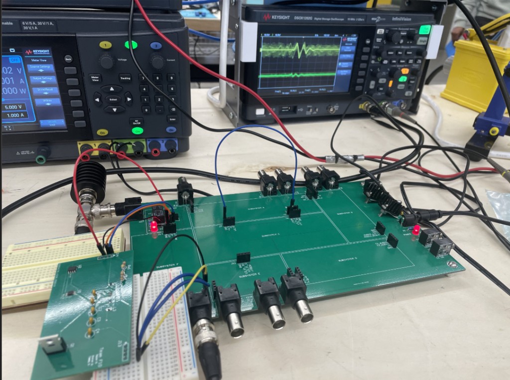
TX Power Amplifier & Filter
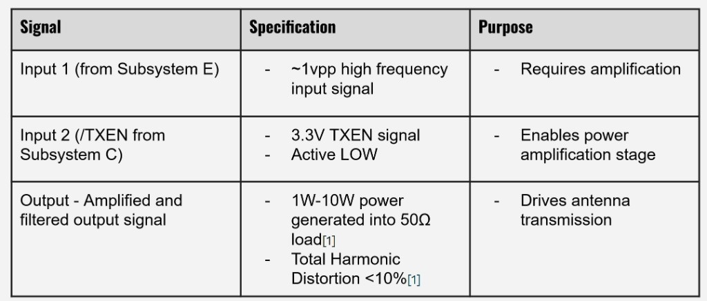
this was subsystem F of a software-defined radio: the transmit power amplifier and filter, built by team F10. it sits at the end of the chain, taking a roughly 1 vpp high-frequency signal from the previous subsystem, amplifying it, and filtering it so it's clean enough to drive an antenna.
the requirements set the targets. generate 1 to 10 W into a 50 Ω load at 14 MHz, keep total harmonic distortion under 10 percent, only enable the amplification stage when the active-low /TXEN control line is pulled low, and fit everything inside a 2000 mil by 3550 mil (50.8 mm by 90.2 mm) board.
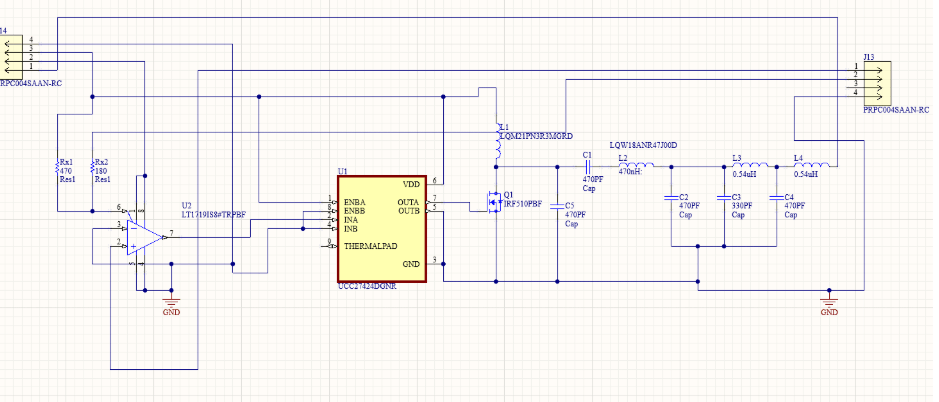
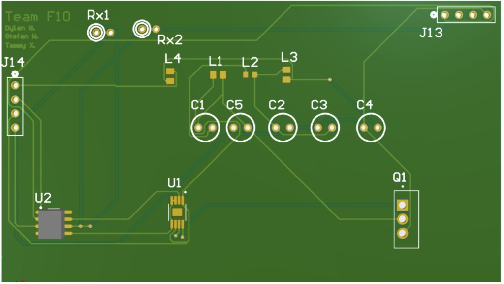
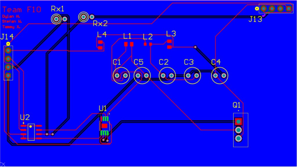
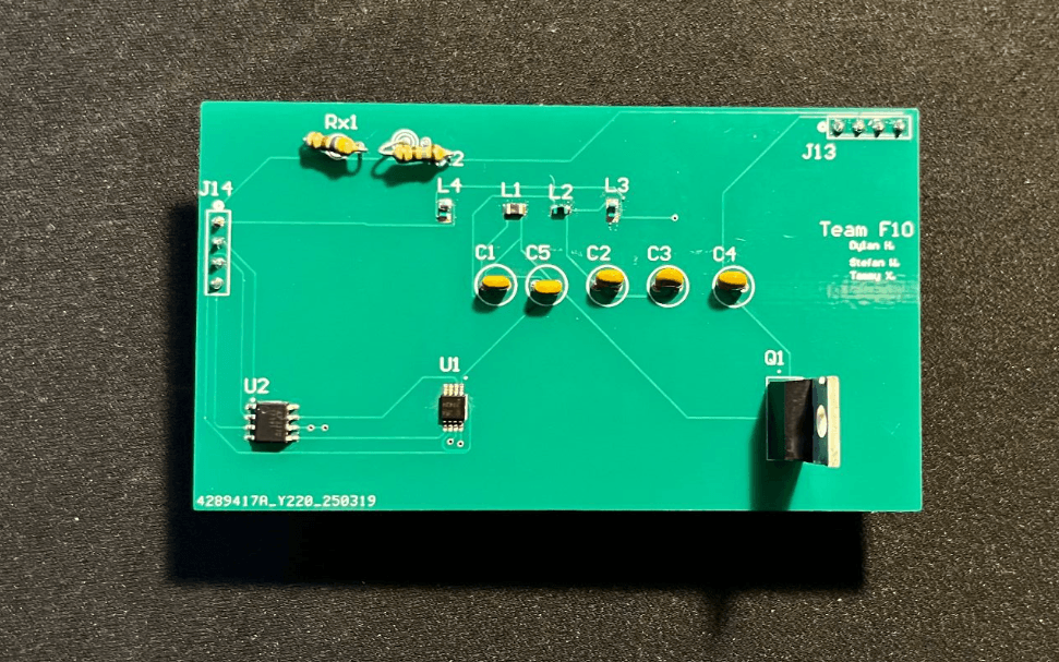
the topology is a class E power amplifier. an LT1719 comparator (U2) squares the incoming signal, a UCC27424 gate driver (U1) drives an IRF510 MOSFET (Q1), and a multi-stage LC low-pass filter (L1 to L4, C1 to C5) cleans up the output before it reaches the 50 Ω load. i designed the schematic and PCB in Altium and had the board fabricated and soldered.
testing ran in two stages: first the assembled PCB on the bench, then breadboarding the individual stages once the breakout boards were available, so each part could be characterized on its own.
the class E amplifier stage matched its LTspice simulation when driven with the equivalent test input, confirming the amplifier behaves the way it was designed to. on the output side, an FFT of the signal measured a THD of 1.933 percent at the target 14 MHz, comfortably under the 10 percent spec, which shows the low-pass filter is doing its job and attenuating the unwanted harmonics.